
3. Microprocessor-based system
Introduction 1. Some examples of timing of Z80 2. Decoding of addresses 3. Diagrams of a microprocessor Z80 board 4. Information processing systems 5. Types of memories
Let us start by examining a small processor electronic schema. This diagrams represents a processor, a RAM memory and an interfaced circuit.
The microprocessor (also called CPU for Central Processing Unit) is the principal component of a computer, it executes a list of instructions, without any decision of its share. These instructions lists are commonly called a program. Each models of processors reads specifics instructions from its design in the form of a basic language which one calls assembler. This programming language is complex to use since it is specific "machine" and coded into hexadecimal (as well as the data what still complicates the programming). The current softwares are written in advanced languages (C, Visual BASIC...) which transpose the programs into comprehensibles instructions by the processor. Except some small improvements, all the microprocessors of the computers of the X86 family include/understand the same assembly language (Pentium, Athlon...). The processor does not make any decision, only conditional instructions are influenced by external situations: keyboard, request for service of a peripheral...
The interfaced circuit represented above is varied: memory, I/O ports, ... Nevertheless, all the electronic microprocessor assemblies include a starting program in ROM memory (the contents are not deleted without supply voltage of the circuit). This program makes it possible the microprocessor to carry out its initiation with starting (what it must do like detecting the hard disk, to test the memory...). A microprocessor-based system thus consists of several interfaced circuits, for example, ROM memory (obligatory), memory RAM (working memory for the results), wearing of entry (keyboard), wearing of exit (bill-poster)... put in parallel.
Two types of processors are manufactured, the microprocessor and the microcontroller. On the level data processing, the 2 are practically equivalent. The distinction comes from the established functionalities. A microcontroller is dedicated to inputs/outputs treatments. Some I/O ports are added (in parallel and/or series according to the models) which will make it possible to receive or to send information of slow peripherals. One could use a microprocessor for the same functions but this would require to add external components for each external control. A microcontroller often includes the programming of manner internal in a memory of the ROM type and even of the working memory of the type RAM. As a microcontroller manages slow peripherals, it is not optimized for the speed of treatment of information, nor to even manage large quantities of memory.
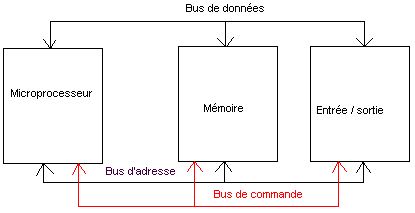
The processor's interface uses 3 systems bus: a data bus, an address bus and a control bus. A bus is a whole of lines of communication (materialized by wire) which connects 2 (or more) digital circuits between-them.
Each memory emplacement or internal peripheral is indicated by address specific (sometimes several following the other, which one calls a beach of address), similar of an postal address. A specific address cannot be divided between several circuits. The address bus makes it possible the processor to communicate with the peripheral via its address (or its beach). An address bus consists of several lines. An address bus 8 bit corresponds to 8 lines of addresses and can thus address 2 8 different addresses, that is to say 256 different addresses, and so on. The higher the number of line of address is, the more the processor is able to manage peripherals. Internal structure limit the max numbers.
Once the peripheral contacted via the address bus, the data bus makes it possible to transfer from the binary data (including the lines of instruction out of assembler): in reading (given transferred to the processors) or in writing (sending of data towards the peripheral). The data bus consists of a certain number of lines. All the capacities of the data buses are indicated under 8 lines of data (in Byte - byte), or in multiple of 8 bits, the current processors use 64 lines of data for example. Thus 1 MB of memory means 1 MB under 8 lines, that is to say 8 Mb (Mega bits).
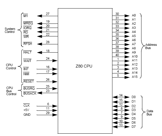
Z80 processor Pin configuration
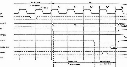
A Control bus synchronizes data transfers between processor and peripherals (memory, inputs/outputs). It ensures the dialogue necessary for the transfer of the data at (operation of writing) or to (operation of reading) the address indicated. The signals of the bus of order also make it possible to manage the interruptions, orders specific which make it possible an external circuit to announce to the processor which it is ready to receive from the data of outside for example. Low signal means that it is active when the signal is to 0 V (one indicates it by signal), not credit when the signal is in a high state (typically 5V). The sequences present on the bus of order are also specific to the processors. It is what one calls the TIMING. Here for example the timing of a Z80.
A0-A15: address bus, exit 3 states, active signal high. 16 bytes allows 65536 different addresses (216). During the REFRESH of the memories, the 7 bits low contain the address of refresh validation. Refresh will be explained with the memories.
D0-D7: data bus, input/output 3 states, active state high
MREQ: Memory Request, left 3 states, announces that the address bus include a valid address for an access in memory (reading or writing).
IORQ: Input output request, left 3 state, active state low, this signal of request for left entry indicates that the low half of the bus contains a valid address of input/output for an operation of input/output in reading or writing.
RD: Memory Read, left 3 active state low. The signal indicates that the microprocessor wants to read a data in the memory or an input/output.
WR: Memory Write, Left 3 states, low level. Indicate a request for writing in memory or input/output.
RFSH: refresh, output, low credit, indicate an refreshing address on the 7 lower bits of the boxwood of address.
HALT: Exit, Stopped state, low level, indicates that the CPU has just carried out an instruction software HALT and awaits a or not Masquable interruption. During the stop, the CPU refresh memories.
WAIT: make an stait, input, low level, indicates to Z80 that the peripheral is not ready to send data, allows to synchronize a slower peripheral.
INT: interrupt request, input, active signal low. This signal of request for interruption masquable (by software instructions) announces to the processor that a peripheral requires an interruption. When the processor accepts the interruption, a signal acknowledgement of delivery IORQ is sent to the beginning of the cycle of instruction according to.
NMI: Non-masquable interrupt, input, started by downward side. This request for interruption at the priority on int and is always taken of load at the end of the instruction in progress. In the case of the z80, the CPU automatically starts again with the address 0066 hex. The contents of the instruction counter are automatically safeguarded to take again the program after the interruption.
Reset: reboot strapping, input, activates low, initialize the processor of which initialization of all the meters, handing-over with 0 of the interruptions. The processor starts again at the beginning of its program of initiation.
BUSRQ: Bus request, makes it possible to use the DMA (direct memory access). The CPU makes pass all its entries left three states in this mode as of the end the cycle machine in progress. This makes it possible the peripherals to entirely take the control of the buses and to transfer from the data towards the memory without passing by the processor. This function is largely used in the current systems (hard disks E-IDE and SCSI, drunk AGP and PCI...)
BUSAK: Bus acknowledge, output, low level, indicate that the CPU accepts the BUSRQ and that the lines are in 3 states.
M1: machine cycle M1, cycle machine in progress is the search cycle of an operational code, this is specific to Z80.
Clock: this signal coming from outside will give rhythm the whole of the signals of the assembly. It is the work frequency of the processor.
Few of these signals really do not intervene in the current concepts on PC systems (and others modern computers). Five signals are however of primary importance for an information processing system: RESET, INT, NMI, BUSREQ and BUSAK. They will be used in the continuation of the course on the level of the PC.
For comprehension, let us make a similarity between a microprocessor-based system with a class room. The professor represents the microprocessor and the students, the peripherals. At the time, only the processor (professor) dialogue with the peripherals (student). A student wishes to put a question, it will use a request for interruption (for example hold up the finger). To locate which student puts the question, the professor will use a table of address (correspondence number of the interruption - addresses student) to distinguish which requires among the others. Once the student clearly identified, the data bus will use to transfer information (the question). Next of the dialogue will use the address bus (distinction of the interlocutors) and the data bus. Let us suppose that the director come in the room. This director can be seen in 2 manners, as an interruption not masquable (identical to a normal interruption but the processor cannot forget to answer, to mask the question). Rather let us see this director like a request for bus (Direct Memory Access). The director (a peripheral with influence) request word (a BUSRQ). The professor finishes his sentence in progress (the instruction of the processor) and announces to the peripheral (directing) which it gives control by a BUSACK (that it releases drank them while being disconnected) and the peripheral - director will be able to speak on the electronic assembly (the class supplements or a pupil - particular peripheral).
... that will make me odd when a student puts a question (forgiveness a request for interruption).
3.2. Some examples of timing Z80 microprocessor
The purpose is not to return in the details of the TIMING of Z80 (nor of another besides) but to explain what occurs in the heart from the microprocessor assembly.
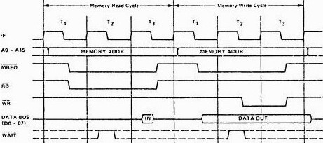
Read/write memory
Diagram represents loading of an instruction or a data by the followed processor of a writing. The whole of the signals is given rhythm by the clock. The microprocessor starts by putting a valid address on the address bus (that where the instruction is). Once the stable signal, it emits a signal MREQ and a READ to announce to the memory that a valid address is present on the bus and that it will ask an access report in reading. With the end of the cycle, the memory transfer on the data bus information (IN). In the case of a writing towards the memory, signal READ is replaced by a WRITE signal. A signal WAIT is returned by the memory (or more generally by a small assembly inserted in the control bus) to slow down the assembly.
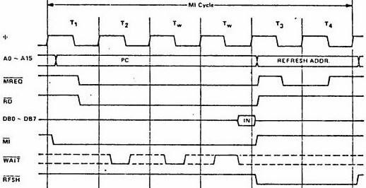
Instruction of Fetch code with Wait States (instruction of loading of data with 1 latency).
This timing is identical to that above except that 2 latencies (WAIT) are inserted to slow down the assembly (case where the memory is not fast enough for the microprocessor) and a REFRESH signal is sent to the end of the loading of instruction.
Request of interruption.
An interruption makes it possible a peripheral to announce to the processor which it must occupy of him (arrived of a data...). INT signal is sampled by the processor on the rising side of the last cycle of clock of each instruction. This signal of interruption is accepted only if the mask software of interruption (a specific order assembler which requires of the processor not to hold account of the interruptions masquable) is not accepted or if signal BUSRQ is not active (request for DMA).
When the signal is accepted, a M1 signal is generated. During this special cycle M1, signal IORQ becomes active (in the place of the signal report MREQ), indicating that the peripheral requiring an interruption can place a data on 8 bit on the data bus. In the case of Z80, 2 instructions of waiting of office are generated, which avoids an electronic assembly to slow down the reading of the data on peripherals slower than the memory. This makes it possible the signal to be stabilized.
3.3. Decoding of addresses.
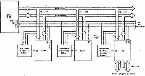
Z80 microprocessor address decoding
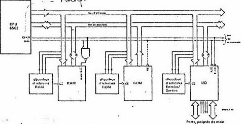
6502 microprocessor address decoding
Above the address decoding for Z80 and one 6502. The signals Read/Write are decoded differently. Z80 has the pins READ and WRITE, with the difference of the 6502 which does not have that a pin read/write. We connect each time a memory RAM (random Memory Access), a ROM memory (Read Only Memory) and a peripheral of exit.
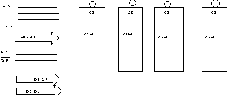
Exercise: let us suppose systems address bus 16 bits, data bus 8 bits comprising 4 circuits reports comprising 214 valid addresses each one on 4 bits of data. Draw the data and address buses, as well as the decoding of address on terminal EC (Enable Chip) containing NAND, OR or NO gates.
3.4. Diagrams of a board with Z80 Microprocessor
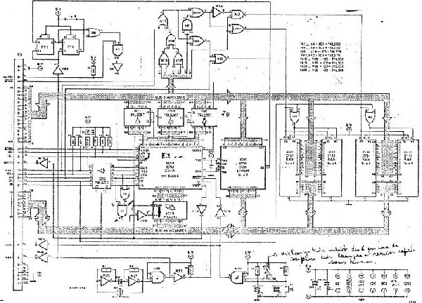
Into diagrammatic, the diagrams (without power supply) becomes like below.
z80 processor is connected to the address bus and the data bus using tri-state buffers. These buffers are not obligatory (included in the processor) but are often added by precaution. These buffers "three states" allow the functions of DMA (Direct Memory Access) of the electronic assembly: direct transfers of the data of (or towards) the memory starting from a peripheral circuit without transit of the data by the processors. The peripheral circuit must with this intention control the three buses.
Address bus is connected with low adress to memories and peripherals. The high adress part is reserved for decoding of address.
Data bus is connected on all the peripherals witch are also connected to the command bus with signals commands reading (READ) and writing (WRITE), low enable.
RESET signal (identical as that on the front face of the PC) initialize the assembly in manner hardware. In opposite to RESET software (< ALT > + < CTRL > + < Del > which is used by the operating system), this functions ca be used in all the planting cases, except if the electronic assembly is in fault what is rare (Microsoft contributes definitely more better to PC's problems than INTEL, VIA, AMD and all the others hardware manufactured).
The last is the clock signal which synchronizes the speed of all transfers between all the circuits.
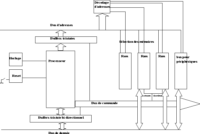
3.5. Data-processing assemblies
The diagram above represents a microprocessor-based system of the industrial type. Very effective in a "closed" process, it is not easily usable just as it is in an information processing system running. All work will be to replace the peripherals by more or less specialized circuits.
In the case of a computer, it will be necessary to post the result of the work of the system on a screen or a LCD. In the case of a computer, one uses a dedicated circuit inserted on an electronic board which one calls "graphics board".
So that we, users, can communicate with the computer, we will insert a keyboard and a mouse. Those are also connected via an one-way circuit.
In the last, to be able to interface various ancillary equipment, we will use "wearing of communication". These ports can be parallel type or series.
In the case of a parallel port, the lines of data are multiple 8 (at least in an information processing system of type PC or MAC). They is wholesale a continuation of a data bus towards outside via a dedicated interface which uses signals of control more specific to the ancillary equipment. The connection of a printer via a Centronix port is of this type.
In the case of a port series, the transmission of information is done via a wire (in practice 3 minimum: sending, reception and mass). Information on 8 bit (one Byte) is cut out to send each bit one following the other. It is the case for example of a modem (port series), of a peripheral USB. The wire of communication receives not only the data, but also of the signals of control. We will see in detail these connections later.
In the last, the system above is called closed system. Indeed, it is not possible to connect on this system of the additional boards. In the case of opened systems, as it is the case for the PC, one installs on the board of the internal ports. They have nothing to do with the wearing of communication above. In fact standardized connectors (dimension, stitching, timing of the signals...) make it possible to insert additional electronic boards for dedicated functions, in particular of the wearing of communication parallel or series.
3.6. Types of Memories
2 types of memories are used: ROM (Read Only Memories) and the RAM (random access memories).
A memory RAM allows the writing and the reading. Nevertheless, it requires to be refreshed regularly. Indeed, the data (1 or 0) are safeguarded by capacitive effect in a transistor. The RAM are connected by outside by the address bus and the data bus. The signals of control are EC, WR and RD (oe). Moreover, and it is there their principal problem, the contents is unobtrusive if you cease of fed.
A ROM memory is only reading and directly programmed by the electronic circuit manufacturer. The contents (program - data) are thus not modifiable. So of other circuits of the ROM type modifiable are used: Eprom (Electric PROM) programmable in 1 time (but beings in certain versions erased with light UV can), EEprom (Electric Erasable PROM), which one can erase completely several times and Rom Flash that one can write directly by an electric signal. All these circuits keep information if the supply voltage is out.
The BIOS (or UEFI), the Rom electronics of the PC comprising the electronic program of starting, this memory is of Rom Eprom type or Flash. This BIOS appeared with the computer containing microprocessor 286 of IBM. Bios is programming specific to the PC and allows some parameters specifics users. The parameter settings users are safeguarded in a memory. This Ram memory (the contents disappear if the circuit is not fed) is supply permanently by a pile.
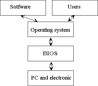
One indicates the programming specific to electronics under the name of firmware. This last concept modifies our basic diagrams of processing. The flashage of the BIOS thus makes it possible to put in the part "flash Rom" a new version of the firmware of your computer. During the operation, the firmware part is charged in memory RAM, time to reload in ROM memory the new version: if there is an interruption of current during this operation, it is impossible to start again the motherboard (and thus the computer), the BIOS (the ROM part of a system PC) being absent or incomplete.
|
Next chapter for hardware 1 training > 4. Performances of a microprocessor-based system |
| < 2. Base of electricity for technicians. |
The hardware training 1: computer and peripherals. The Hardware 2 training: networks, communications and servers
![]()