7. Processors internal structure
1. Internal structure of a basic processor - 2. Cache Memory - 3. Passage of the CISC to RISC - 4. Pipeline architecture, superpipeline and superscalaire - 5. Cut and power supply of the transistors - 6. Internal structure of the processors - 7. Structure of Athlon 64 and Athlon XP
In chapter 5, the processors were analyzed by type (family, manufacturers). This chapter will explain the internal architecture of these processors. To know the internal structure of each processor in detail would be complicated too much, but this will make it possible to clarify these differences in performances of the processors for an equivalent speed.
All "processors PC" use the same instructions as first 8086 CPU of INTEL (but often the operating system is not compatible any more with these old programs). The instructions which a processor is able to read are programmed out of assembler language. All the operating systems and programs are re-coded starting from advanced languages (C, Pascal, Visual BASIC...) towards this assembler. If a new processor uses the same basic instructions as a processor of the first generation, this is not restrictive. In the course of evolution, some instructions were added to allow addresses decoding on a higher beach (386) or for multi-media instructions (Pentium MMX, Pentium III, K6-2 and K6-3).
Obligation to keep the basic instructions of the 8086 for the processors according to installation of serious problems for the design of new compatible microprocessors X86. The instructions of the 8088-8086 are not frankly easy. Coded between 1 and 5 bytes, they do not make it possible to predict space used by the following instruction. According to a coding with 8 bit of the instructions, an instruction can take several bytes.
Processors 8086-8088 (and olders) have a structure called types CISC (Complex Instruction Set Computer). The first originators of processors added the most possible instructions to allow the user to polish his programs. Nevertheless, these multiple instructions slow down the operation of the microprocessor and are used little in practice. Currently, processors RISC ( Reduced Instruction Set Computer) are used. The number of instructions is reduced, but carried out definitely more quickly. Each complex instruction can be programmed by several simple instructions. The current technique is to give the responsibility of instructions CISC 8086-8088 to re-code them in faster instructions RISC.
1. Internal structure of a basic processor
Let us take again our Z80 and distinguish the various parts: with the top, an internal bus of data, below an internal bus order and a bus interns of address. Knowing the diagram of the microprocessor-based systems, this is not astonishing. In the part of right-hand side, an UAL (Arithmetic Logic Unit). This UAL is a calculating unit, it is connected to a noted buffer memory the accumulator and through bus to a whole of memory called registers. In our case, these registers are noted B,C, D... The registers A', B', It... is specific to Z80, but also exists in the 8088. This makes it possible to work with two zones memories which one makes rock. The UAL of left makes it possible to make calculations on addresses. Notice the small incrementor +1 who allows to increase the pointer programs (the address where the next instruction of the program is).
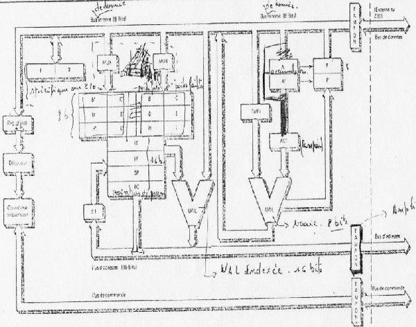
The diagram of the processors of this generation showed the following diagram:
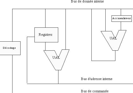
This structure charges an instruction code at the same time, that is to say for an instruction of the type LDA XX XX (loading in the accumulator of the data contained with the address memory XX XX), three cycles of instructions (for LDA and 2 for the address). This condition moreover is met only if the processor charges an instruction by cycle of clock, but it is the case in a system INTEL. As the instructions of the processor current are compatible with the 8088, the sizes of the registers are it too. It is thus impossible to increase the size of these memories to increase the speed of execution.
Which are the possibilities of increasing the speed of a processor without modifying the structure?
- to carry out several instructions at the same time, but that is difficult since certain instructions are conditional.
- to make pass via one to decode the instructions of the type CISC in faster RISC.
- To make sure that the processor never awaits instructions, that they are directly accessible.
- to increase integration by decreasing the size of the transistors. This increases the speed of transfer between the various parts.
All these tricks are currently used, as well by INTEL, as by AMD and Cyrix (VIA).
2. Use of a cache memory
While inserting a fast buffer memory between the processor and the memory (slower than the processor), one allows the processor to quickly reach data and instructions which it often uses. One distinguishes internal L1 cache (established in the processor) and a L2 cache (external with the processor, even if it is established in the same case, case of Pentium II, K6-2 and K6-3 and following).
Various cache architectures
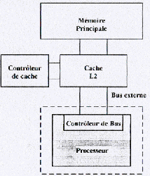
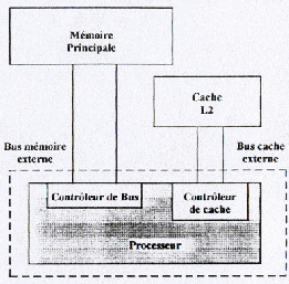
Structure 486, Pentium, K6, 6X86 - Nexen NX586 structure
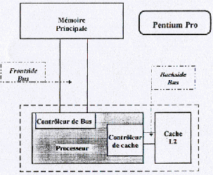
According to type of processor, the L2 cache is managed differently. In the case of Pentium Pro and Pentium II, the L1 cache is not any more out of direct plug between the memory and the processor, but directly to manage by the processor. The cache is established in the same case for these processors.
By way of example, a CELERON 300 without L2 cache is 40 % lower in performance with Pentium II of the same frequency and of identical structure.
Moreover, the current processors use 2 internal L1 caches: for the data, for the instructions. More the cache size increases, more the difficulties of managing this cache memory increase, but more speed increases.
3. Passage of CISC to RISC
Another solution to increase the performances is to make pass the structure of the instruction of the CISC (instruction 8088) in RISC. Each firm uses in-house its own instructions, better is this transfer, better are the performances. This explains why the effective speed of a processor is not identical for 2 of the same processors frequency, but of different structure.
|
Favour CISC processors: |
Defaults of CISC processors |
|
. Instructions closer to a high-level language . Programming more compact . Faster and more elegant writing of the application . Less occupation memory of the programs . Execution requires less bytes report |
. far too many different instruction codes.
. cut instructions high and variable (1 to 15 bytes - bytes by
instruction) |
|
RISC Microprocessor |
|
Clear separation enters the instructions of access report and the others Standardized instructions, in the face and execution time Unit of decoding cabled, not microcoded architecture superpiline, superscalaire Very many registers with General uses One or more internal(s) cache (s) as well as internal plugs and an instruction set reduced to the simple instructions. |
|
Each modern processor will seek packets of X86 instruction, decodes them on several lines of 8 bits to make them pass in instructions RISC. This poses problems at the time of conditional instructions. How the processor can charge several instructions and carry out them according to the choice not envisaged at the beginning? Each originator uses either a circuit of prediction located upstream of circuit of decoding CISC - RISC (case of INTEL), or a table of connection which memorizes the last connections (AMD). As the instructions are charged a long time in advance, it may be very well that the data are changed...
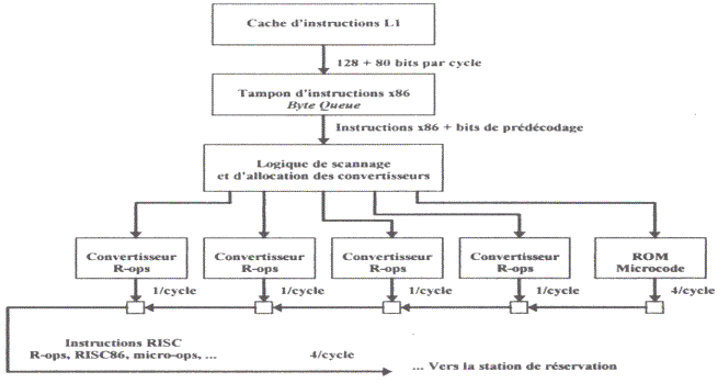
This change of the type of instruction also made it possible to establish one (or several) calculating units specialized in floating point (real numbers) within the processor. This calculating unit is the mathematical processor. This coprocessor is used in the specific calculations, used mainly in technical drawing and plays.
The passage of processors RISC to processors CISC brought other internal changes, we will review them.
4. Structure pipeline, superpipeline and superscalaire
In the 8088-8086, the processor began the treatment of the following instruction only when it had finished the preceding one. The use of a structure pipeline allows the treatment of several instructions at the same time. In the case of a structure pipeline, the execution of an instruction is broken up into:
- loading of the instruction in the processor
- decoding
- execution of the instruction
- reference of the result
As only the first and the last instruction use the external buses, the cycle of the following instruction can start at the same time as the internal decoding of the instruction. This makes it possible to carry out several instructions at the same time.
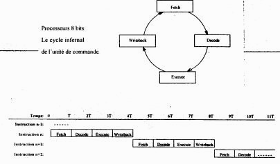
Structure standard
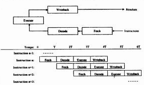
Structure PIPELINE
In superpipeline architecture, instruction execution is now divided by 6. The number of simultaneous execution is hardly higher in super pipeline compared to an architecture pipeline in the instruction usual. On the other hand, as of time used by each part of instruction is weaker, each time that a part is omitted (because not necessary) the execution is even faster for the following one.
Super pipeline: the processor does not treat the instructions of only one blow, but in 6 stages: pre extraction, decoding of instruction (2), execution, generation of address and differed writing (case of a loading towards or of the memory).
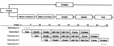
superpipeline structure: the M1 processor of CYRIX, architecture go up to 7 levels.
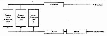
Structure super scalar
In the internal structure of processors super scalars, the processor includes several units of execution of instruction which work at the same time. Athlon is super pipeline and super scalar.
5. Most transistorr.
Currently, the microprocessors use CMOS or BiCMOS transistors . The more technology progresses, the more the supply voltage and the transistors size decrease and the more the number of transistors increase. A reduction of the size of the transistors decreases the distance from transfer between 2 information and thus less thermal dissipations (since the signal follows a shorter distance, less heating in the processor). Moreover, the complexity of the current processors increases the number of transistors.
In 1995, transistor size was 0,5 micron. In 2003, it is 0,13 micron with Pentium IV superiors 1,7Gh and last athlon.
If since Pentium MMX, one passed to power Bi-voltages, the supply voltage also decreases since that of K6-3 to 450 MHz is currently of 2.2 V Attention, systematically check the tension on the processor and not on the motherboard or in the technical notes of this one. For the processors Bi-tensions, to take V Core , even if the second tension is posted.
The modification of the tensions of the processors arrived with the first 486DX2 of Cyrix (but became general). All the former models used the 5V. A power error on a processor involves its destruction shortly.
6. CPU Internal structure
While adding some with above advanced, one arrives for example at K5 2,5 times faster than one 486 of the same frequency. Briefly let us analyze some internal structures of processors. Let us start with K6-2 of AMD above.
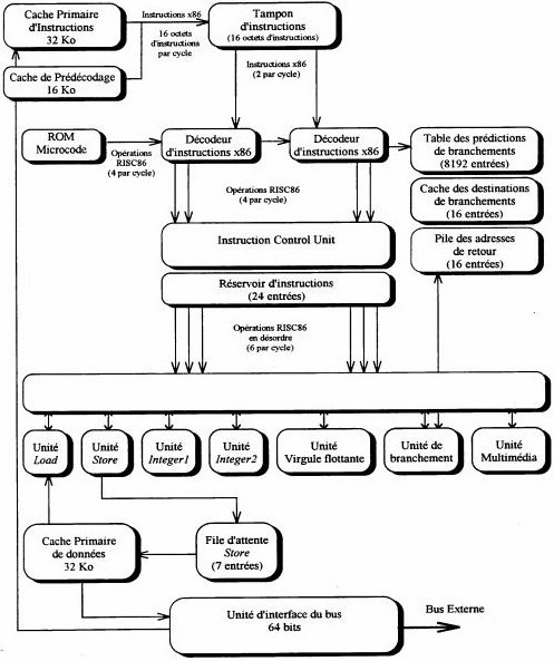
Diagram of general architecture of a AMD K5
In top on the left, the L1 instruction cache (the data cache is in bottom) by which forwards all the instructions coming from the memory (case of the AMD). The system below predecodage is used to check them the type of instructions which arrive (memories or execution) and is used for the predictions of connections. The whole is connected to a plug of instructions which sends 2 X86 instructions by cycle of clock towards 4 decoders of instructions (passage of the CISC with the RISC) This decoding is carried out by the Rom Microcodes. Instructions RISC are transferred towards a table from predilection from connections, associated another cache. Other share, the instructions are treated in RISC by the Control instruction Links which also sends the instructions starting from a tank of 24 orders RISC86 towards the various parts below: Load and Store (management memories), two units of entireties and one of floating point, a unit of connection which also manages the table of prediction and a multi-media unit related to instructions MMX. The whole is connected to the external data bus via the data cache and the Unit of interface Bus which also manages instructions cache. That of Pentium Pro below is identical, with share the external L2 cache which is not connected directly to the memory. This structure is included in Pentium II and Pentium III.
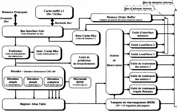
General architecture of a processor Pentium Pro (identical to Pentium II and III).
7. Structure of Athlon 64, 64 FX, Opteron and athlon XP
8. Conclusion.
The modification of the internal structure of the processors returns the performances of a processor rather difficult to check while being based only on the frequency. This explains commercial do-it-yourself of Cyrix which systematically indicated speeds of its processors, not by effective speed, but by speeds of comparison compared to equivalents INTEL according to Brenchmarks (though). AMD with Athlons XP and Sempron makes in the same way. If the number of instructions decoded at the same time should further increase, the current direction of the processors goes towards the reduction in the size of the transistors, which leads to possibilities of increase in frequency. Indeed, more the number of transistors increases, more dissipation of heat is important. But the more the size of a transistor decreases, the less this dissipation is important. Other materials are in the course of use, IBM uses already internal drivers coppers some, whereas current technology is based on aluminum. Copper is better electric conductive (then less dissipations) but requires a higher technology, with difficulties of more important integration. This does not avoid in any event not the ventilator on the processor.
In relation:
- Course: processor PC Processors used in the PC
- Installation of a mother board and processor: Hardware course, chapter 22
- Microprocessor based system Operation of a microprocessor-based system
- Microsoft Operating system: technical training in same way: course for techniciens on DOS and Windows
| The continuation of the course hardware 1 > 8. Chipset PC |
The first year hardware course (computer and peripherals). The second year hardware course (networks, servers and communications)
Competences with the service of quality in data processing.
