
5. Processors for PCs
Introduction - 1. 8088 and 8086 - 2. 286 - 3. 386 - 4. 486 - 5. Pentium - 6. Pentium MMX, K6-2 and K6-3 - 7. Pentium II - Pentium III and Celeron - 8. Pentium III Coppermine - 9. AMD Athlon, Duron and Thunderbird - 10. Pentium IV - 11. Pentium 4 EE - 12. Sempron - 13 Microprocessors 64-bit - 14. Athlon 64-bit AMD - 15. Intel Core, Core 2 and Core 2 Duo - 16. Intel I7 - 17. Intel I5
This part is divided into 2 parts:
- PC microprocessor computer desktop: historical and current processors, technology.
- the CPU servers (Pentium Pro, Xeon, Itanium and Opteron)
The Processor (microprocessor) is the component hardware as most important from a computer. This component is the unit of data processing. In itself it is unable to perform any action. Its work was limited to read programs (sequences of instructions in assembly language), to decode and execute. It takes no action, simply run "stupidly" what is asked. This is the software with conditional statements which is responsible for "intelligence" of computers. To its advantage, It performs these tasks without error and quickly. For an introduction to electronic circuits based processor
The 4004 is the first microprocessor, manufactured by Intel for a Japanese manufacturer of calculs machine. It refuses to excessive size (dimension). Intel puts then on the market without conviction but with the success that we know. The 80s saw the emergence of Zylog Z80 (compatible with standard instructions with the 8080), 6800 Motorola (including the following have been used also by the MAC), the 6500... With the arrival of XT IBM and the use of 8088 (8086 for compatible PC), Intel became the first manufacturer late 80s.
The processor family Intel compatible have evolved. Before considering all the hocus that designers of microprocessors currently use to improve performance (structure of microprocessors), A little history of models used in PCs and their characteristics.
1. 8088 and 8086.
First microprocessor family PC (Personal Computer), the 8088 (used by IBM) uses an internal data bus of 16-bit lenght, but 8-bit external. The 8086 (used copies of the PC XT), fully compatible with standard instructions, had a data bus full of 16-bit.
The PC was released in 1980 under the name of XT. Due to its original design (despite its high price), the XT had many advantages over the competition.
-
Bus device (connectors to implement maps) type 8-bit ISA. This is called an open system.
-
Memory Capacity extensive socket. A Commodore 64 and similar included in Office 64 MB of memory. The XT could accommodate 640 MB, even if the purchase, the capacity was lower.
-
The OS Not in ROM, but located on a floppy disk. And here's the real beginnings of Microsoft in operating systems with Dos we shall see in operating systems.
-
A large portion of the addresses and interrupts in the PC are standardized, including future peripherals. With the introduction of the ISA bus, an address range is reserved for peripheral cards, one for the memory. This can change the map screen without replacing PCs.
As the electronic diagram of the motherboard was based circuits TTL very common (74LS), copies of this computer were easy, this is called clone, and currently: white PC, OEM, ...
2. 286 (80286).
Two years later, IBM released the AT, based on microprocessor 286 from INTEL. Performance Awards (frequency from 8 to 16 MHz), the data bus is totally 16 bits. The ISA bus also goes into 16 bits.
IBM implements some new features like a clock (RTC - Real Time Clock), one BIOS on EPROM and Setup, backed by a battery. The BIOS is the firmware of the PC and acts as an interface between the electronics of the PC and operating system. Unless some UNIX operating systems in the early 80s, all pass through the BIOS to retrieve information.
Memory is also changed. It is no longer composed of smaller components that are added, but a memory bank covering the entire memory range lower than 1 MB, also the memory areas reserved for so-called high memory.
3. 386 (80386).
1991, here begin the real improvements in the structure and the beginnings of Intel, in marketing under competition from a new concurrent named AMD who made the Intel license.
INTEL released first the 386DX-25 and 33 Mhz. Its data bus is 32 bits internally and externally. As its price is high and memory Ram expensive, Intel released a smaller version, the 386SX with a craft similar to 8086, data bus internal 32-bit, but outside of 16 bits. AMD released its first 386DX with a little delay, clocked at a frequency of 40 Mhz, fully compatible with the 386 to INTEL.
Motherboards with memory external cache L2 are emerging. This faster buffer than normal memory keeps the lines of data and programs most often used to refer to the processor more quickly, this improves performance.
80386 uses 3 modes
-
Real Money (Real): the processor works as a simple 8088, the same method at 286.
-
Protected Mode (protected): The microprocessor can use all the possibilities of 80286, more specific instructions from the 386 with a memory addressing up to 4 MB
-
Virtual Mode (virtual), emulates several sessions of 8086, used from Windows 95.
Intel also offers a specialized processor for 80386, the coprocessor mathematical 80387. This component is specialized for floating-point. This increases performance for games, technical drawing, ...
4. 486 (80486).
INTEL released the 486 DX with a socket 1 the first with the math coprocessor directly implanted into the microprocessor. This circuit is dedicated to floating-point calculations (real numbers). The L2 cache external capped at 256K. The frequency begins at 33 MHz, to 50 Mhz. To reduce prices, Intel released the 486SX: same 486DX, but without math coprocessor integrated.
When AMD comes with a 486 at 40 Mhz, Intel's first CPU multiplier, the 486DX2-66. These processors use an internal multiplier, for all the following processors will be external. Except for the supply voltages possible and type (brand), you can directly replace a 486 DX33 with a 486 DX2-66 (external speed is 33 Mhz). For 486DX4-100 where we could use 33 X 3 40 X 2.5 or 50 X 2, the choice is made obligatory on the motherboard. Attention a DX4-100 Intel can not be replaced directly by a DX4-100 from Cyrix or AMD.
With the 486, INTEL takes over with its math coprocessor and thus performance
Since the 486DX2, processors therefore use 2 frequencies, one internal (frequency reference) and an external bus, called FSB (Front Side Bus). The supply voltage is more than 5 V, but rises to 3.3 V. The other models are DX2-50 DX2-66, DX4-80 and DX4-100.
Since the 486 DX2, all modern microprocessors must be fitted with cooler and fan. Computers brand often used simple radiators up Pentium 120 Mhz.
The Bus VLB makes its appearance, is an extension of a few pins 486 on an ISA slot, no compatible with the Pentium, and others.
5. Pentium
Intel offers the Pentium first (the name comes from a commercial protection of the term). Its main feature compared to its predecessor is the implementation of internal cache L1 8 KB for the program and 8 KB for data directly implanted into the processor.
Follows directly in June 1994 the output of a microprocessor with an internal architecture revolutionary, the NexGen 586. His instructions are fully compatible with the Pentium, its faster performance but not the socket (pin). The motherboards are hard to find and ultimately the firm disappears, bought by AMD will call its first "Pentium" Am5x86. It is equivalent in performance but uses 486 boards. AMD will continue with the K5 pin-compatible (and therefore motherboard) with the Pentium, followed by the K6 and Cyrix the 586. The K5 is not very powerful and will quickly be replaced by the K6, which was developed based on the Nexgen 586 (firm acquired by AMD).
The Pentium 60 and 66 MHz using a special socketb, the following will use the socket type 7.
Again, it will have to use multiplication factors between the internal speed and the external (FSB). Instead of the 486 DX2-66, the multiplier must be reported on the motherboard.
The external frequency is related to the speed of DIMMs that time (66 MHz maximum). If choices, more external speed is faster, the PC will be. For example, a Pentium 100: a PC configured with 1.5 X 66 will be faster than 2 X 50.
The actual frequencies, FSB and multiplier are listed on page Features processor socket 7
6. The Pentium MMX, K-6, K6-2 K6-Cyrix 6X86
In May 1997, INTEL add additional instructions in its microprocessor called the Pentium MMX. They are especially dedicated to compression, even if they are listed as "MULTIMEDIA", a term advertising in fashion at the time. At the same time, the Pentium contained an L1 cache of 16 K, the Pentium MMX 32 K (shared equally between the data and programs). AMD adds the same instructions in his K-6. The frequency of the Pentium MMX is 166 Mhz, 200 and 233 Mhz
AMD continues with the K6-2 with the same socket that adds another 21 new instructions (3dnow, Located in DirectX 5.0 from Microsoft) to compete with the Pentium II and a L3 cache in August 1999 in the K6-3. The K6-3 uses an L1 cache of 64K and an L2 cache from 256K to CPU frequency. As with all processors socket 7, the L2 cache is nonetheless always integrated into the motherboard.
| Speed | FSB | multiplier |
| 233 | 66 | 3.5 |
| 266 | 66 | 4 |
| 300 (K6-2) | 66 | 4.5 |
| 333 (K6-2) | 66 | 5 |
| 350 (K6-2) | 100 | 3.5 |
| 400 (K6-2) | 100 | 4 |
| 450 (K6-2 and K6-3) | 100 | 4.5 |
The Pentium MMX, K6 (equivalent to MMX), K6-2 K6-3 and MII Cyrix still use socket 7 with an evolution towards SuperSocket 7, consistent amount that accepts higher frequencies.
The heart of the K6-III
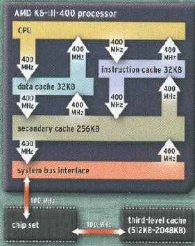 The K6-III AMD has an L2 cache 256-KB integrated One Died at the same
frequency as the processor, either 400 or 450 MHz. In the Pentium II and
III of the time, the secondary cache L2 only work half the processor
speed. The K6-III also include a cache L3Created
by plugging the CPU on a motherboard for K6 II (pin compatible) with
512, 1024 or 2048 KB L2 cache
The K6-III AMD has an L2 cache 256-KB integrated One Died at the same
frequency as the processor, either 400 or 450 MHz. In the Pentium II and
III of the time, the secondary cache L2 only work half the processor
speed. The K6-III also include a cache L3Created
by plugging the CPU on a motherboard for K6 II (pin compatible) with
512, 1024 or 2048 KB L2 cache
The actual frequencies, FSB and multiplier are listed on page Features of Pentium
7. The Pentium II - Celeron and Pentium III.
While AMD prepares the K6-2, Intel released the Pentium II:
- the L2 cache is no longer located on the motherboard but directly managed by the processor and located on its casing. The frequency of the cache is half that of the microprocessor.
- new connector to the insert on the motherboard, slot one. The socket is replaced mid-2000 by 370 (Celeron) and FC-PGA (Pentium III). Adapters allow the passage of a slot one at a socket 370 PPGA / FC-PGA with incompatibilities if the marks adapters - motherboards are different. The FC-PGA is identical to 370, with just a few pin further.
- its architecture is totally RISC
With the Pentium II at 233, 266 and 300 MHz (FSB 66 MHz), the chipset used is the 440LX (440FX for all early models), which manages Ram Dimm to 66 MHz, the AGP bus for graphics card, and hard drives Ultra ATA 33 MB / s. The USB 1.1. made its appaition
When Intel abandoned the Pentium MMX, Pentium II are too expensive, the firm leaves the CELERON for PC low end. Early models do not include L2 cache, with performance very low. The following models in integrating 128K (half), but at the same frequency as the processor. These versions CELERON can be used in dual-processor (same speed and if possible, same batch).
Models Pentium II following are 333 (March 1998), 350, 400, 450, 500 Mhz, ... with FSB (external speed) of 100 MHz. The chipset dedicated is the 440BX, which manages memory DIMM 100Mhz (VIA released the Apollo P6 which manages more than the standard Ultra DMA/66 for 33 to 440BX).
Released in early 1999, the Pentium III (Katmai) are identical to the Pentium II (still Slot 1) but include 70 multimedia instructions additional (SSE). These functions allow to obtain multiple results in one direction.
8. Microprocessor Intel Pentium III Copermine
With the release in late 1999 chipset CAMINO 820i, the Pentium III coppermine are etched in 0.18 micron, using DIMMs 133 (via interface) and DRDRam (Rambus) 300 (PC600, 1.6 GB / s) and 400 MHz (PC800). The VIA Apollo Pro 133 handles SDRAM 133 MHz, the performance increase by 4 to 7% compared to an Intel 440 BX depending on the type of Ram (2 types of memory 133 are proposed, the PC133 and VCM133 to better manage time Wait and are faster).
INTEL fate at the same time 4 versions of the same microprocessor, depending on the size of the burn and speed of the bus outside. Here, for example, features a Pentium III 600 Mhz following letter abutting the code:
| Bus 100 Mhz, etching 0.25-micron (Current) | 600 |
| Bus 133 Mhz, etching 0.25 | 600B |
| Bus 100 Mhz, burning 0.18 micro | 600E |
| Bus 133 Mhz, etching 0.18-micron | 600EB |
All versions do not exist. Pentium III etched in 0.18 micron (Coppermine) operating a memory L2 256K but at the same speed as the processor, for 512k, but at half speed, for those etched in 0.25 micron (former). This gives a transfer rate 9.6 GB per second for EP III E (or EB) at 256 bits 2.4 GB / s in Pentium III 600 normal functioning in 128-bit with half the frequency. The copermine to 133 Mhz are interfaced with the i820 from Intel. It does not Dimm 133 Mhz, but RamBus much more expensive in versions FSB 133.
The last core is Tualatin, developed version of Workstation (1 to 1.33 GHz) with L2 cache It died of 256 KB and version Pentium III S (server, with 512 KB L2 cache), one version of Pentium III officially multi-processor SMP.
9. Athlon, Duron and Thunderbird AMD
Released in May 1999, the microprocessor is the first generation 7. The Athlon is the first head towards the Pentium III performance. It incorporates 22 million transistors cons 9.5 million for a Pentium III Katmai.
What are the characteristics of the Athlon over the Pentium III and above AMD: All first 3 units of computation in real numbers (floating point) to 2 for the Pentium II and III (only 1 for the old AMD). If the unit installed in the Pentium has always been superior to that of K6, 3 units of Athlons are each level of the Pentium III. In addition, 2 units of Pentium III can not work at the same time, 3 of the Athlon, yes!
The second difference is the cache built into the processor:
- L1 cache of 32 kB for the Pentium III, but 128K for Athlon
- L2 cache starts at 512 KB to 8 GB for the Athlon, compared with 512k for the Pentium II and III (128K for Celeron).
Another difference is the frequency of the external bus. The Pentium III is limited to 100 and 133 MHz external bus, the Athlon uses the Alpha technology EV6 Compaq (used by the processors Alpha) To accept external buses at 200 Mhz (rising and downward sides of 100 Mhz), but manages only memories PC133 (DIMMs). It is the transition to DDR memory (Double Data Rate) which actually allows the Athlon to run at full speed.
The first Athlon use Slot A, identical in appearance to the Slot 1 INTEL but the signals (and therefore the motherboards) are different. The Slot A (AMD) and Slot One are not compatible.
9.1 Evolution
Mid-2000, AMD replaces the slot A by the socket 462 (socket A) and offers 2 versions of the Athlon: the Duron and Thunderbird.
The Duron is a version cheap and uses an L1 cache of 128 K and an L2 cache of 64 K at the same frequency as the microprocessor. Thunderbird core also uses an L1 cache of 128K, but the L2 cache is doubled to 256K, both at the same speed as the processor. These processors use an external bus clocked at 100 MHz DDR (Double Data Rate, X2) which corresponds in practice to 200 Mhz. The C model of the Athlon (speed of 1 to 1.4 GHz) using a FSB of 133 Mhz
During 2001, the Athlon Thunderbird is replaced by the XP (name of the Core Thoroughbred) With an internal architecture differently, ensuring less heating, with protection against overheating. The L2 cache is 256 KB with 52 new additional instructions called 3D Now Professional. The external bus (FSB) of XP goes to 133 Mhz. We see that the speed is not the only measure of performance. Since the XP, the actual speed of processors is not one on which they are sold but the equivalent Intel processors. In 2002, a version MP (twin-processor) is placing on the market.
In the third quarter of 2002, the external frequency is increased to switch to 166 MHz with the Athlon XP 2.8 GHz (clocked in fact to 2.250 GHz). This rise causes some compatibility problems with motherboards to 133 Mhz but improves performance.
January 2003, AMD modifies the Athlon with the Core BARTON. This new microprocessor starts at 2500 + (actual frequency of 1833 Mhz). The L2 cache increases from 256 to 512K. Performance to actual frequency equivalent are necessarily better compared with Thoroughbred. Find the characteristics of the Athlon XP
Indications Front Side Bus reproduce the actual frequency of bus EV6 using the flanks rising and falling of the clock. Therefore, an FSB of 133 runs in fact 266, FSB from 166 to 333 and a FSB of 200 to 400. The speed external effective are engraved on the label form letter: C 266, D 333 and E 400.
The Duron peak at 1.3 GHz have disappeared in early 2003. The Sempron replaced the Athlon XP in January 2004. For the first model, only the structure changes, they are identical to the Athlon XP.
10. Pentium IV (late 2000)
In 2000, Intel released the Pentium IV based on a new internal structure, the Netburst architecture. As features:
 pipeline
on 20 levels against 10 for Pentium III and Athlon at the time. The latest
models go up until 31.
pipeline
on 20 levels against 10 for Pentium III and Athlon at the time. The latest
models go up until 31.
- can execute instructions in disorder, especially if the data is not in the cache
- The L1 cache instruction received from now until 12,000 instructions prédécodées in RISC unlike standard models that retain instructions CISC-compatible 8088.
10.1. Characteristics.
- 42 million transistors
- Internal registers still 32 bits.
- New socket PGA 423 (replaced mid-2001 by μPGA 478).
- 144 new instructions SSE2 Managed DirectX 8.0
- Unit calculation amended (2 ALU running at twice the speed internal processor, a unit in "Floating Point").
- Memory L2 cache remains at 256 K (increased to 512 K in early 2002) but is improved, the bandwidth from 14.9 GB / s for a PIII 1 GHz to 41.7 GB / s for a P4 at 1.4 GHz.
- The L1 cache contains only 8 KB for data, but the party reserved the instructions are now kept pre-decoded RISC ( "Instruction Trace Cache"). This cache program can contain up to 12,000 instructions, which is not without consequences for poor branch prediction.
- The bus frequency (external) is 200 MHz, but increased to 400 in early 2002.
- The engraving is 0.18 μ, rising to 0.15 μ in early 2002.
The SSE (Streaming SIMD Extensions) is dated 1999 with the Pentium III. These 70 orders assembler additional use technology SIMD (Single Instruction, Multiple Data), such as MMX or 3D Now!. The SIMD can process in one instruction the equivalent of several basic instructions. The SSE 2 adds 144 new instructions, mainly dedicated to the management of the RAM and cache internal but also handling new data types (integer of 128 bits in 1 cycle and real numbers double precision of 64 bits in one cycle for two data).
As the 3D Now! and MMX, applications must be specifically planned as such to use.
Another improvement of the NetBurst architecture is to execute instructions out of order via sequences of instructions in some parts of programs, the time that another internal unit the end.
Notice the media on the sides of processors for the fan of "large size" since it weighs about 450 gr.
10.2. Evolution
- Mid 2001, INTEL replaces the socket PGA 423 Pin the μPGA 478 Pin, without changing the internal architecture
- Early 2002. The Northwood is the second version of the Pentium 4 (P4N). The first version was code-named Willamette (P4W). Its characteristics are the same as the P4W, except that it uses an etching 0.13 mu.m and has 512KB of L2 cache. It is only available format μPGA socket 478 This version is from the 2.2 Ghz.
- Beginning in November 2002. Intel announces a change in voltage for the processor based on the core C-1 (0.13μ), whether Pentium 4 or Celeron. Instead of a single voltage 1.525 V, these microprocessors can now work in 1.475, 1.5 or 1.525 Volts.
- Early 2003. The Pentium IV 3.06 Ghz included the hypertreading that emulates two processors sharing the instructions to execute internally between the various parties dedicated to the treatment.
- Mid-2004: Socket 775A format FPGA replaces the 478 (a ZIF connector). This is the socket which includes the pine now. Intel also take to change the ratings of its processors.
- 2005 A version Dual-core, Denoted Pentium IV D is also released. Unlike the Pentium IV EE, it does not support hypertreading
Notations of Pentium IV, mid -2004
- 3xx series: Celeron D (external bus of 133 MHz -533)
- Serie 5xx: Pentium 4 with L2 cache of 1 MB (older versions E), from 2.66 to 3.8 GHz
- 6xx series: Pentium 4 with 2MB of L2 cache, 3.0 to 3.8 GHz
- series 8xx: Pentium D (Dual Core) with 2 x 1 MB Level 2 cache, from 2.66 to 3.2 GHz
- Series 9xx: Pentium EE dual core with 2 x 2 MB L2 cache, 2.8 to 3.73 GHz, FSB800 or 1066.
In 2006, the architecture is replaced by the Intel Core, Less energy, but also to go up in frequency. The size of the pipeline is also reduced, decreasing the time latent in the memory transfer.
11. Pentium IV EE
Intel does not develop processor desktop 64-bit (like the Athlon 64-bit). The Pentium IV, even using the hypertreading can not resist the performance of Athlon 64-bit (even in Windows 32 bit). Intel has released an enhanced version of the Pentium IV in late 2003, the Pentium IV Extreme Edition (referred to as core Prescott). His performance is still lower than the Athlon 64-bit AMD. This processor using a FSB of 800 MHz is clearly dedicated to the players. Using a socket 478, so it is compatible with the motherboard Pentium IV normal FSB800 (even if incompatibilities are always possible).
To improve performance, Intel has taken the old recipes. The L1 cache dedicated to data is doubled (16 K to 8 K for Pentium IV). The L2 cache is also improved since going from 512 kB to 1024. The number of transistors rises to 125 million for burning in 0.09 μ.
This is not the only development of this architecture. The pipeline for integer calculations from 20 to 31 floors. Increasing the length of the pipeline has some flaws. As we shall see in the processor architecture, in conditional statements, if the pipeline is loaded instructions A, and that the conditional statement of the program asks the following statement B, the pipeline must be emptied before reload the new sequence of instructions. INTEL has therefore set out to improve in the Prescot this branch prediction.
To complete the picture, the Pentium IV EE integrates SSE 3, 13 new instructions. Like all multimedia instructions, this requires the use of programs recompiled against these new instructions.
The Pentium IV EE (Extreme Edition) is the high-end Intel desktop. Almost all the technological advances of Intel servers (except the 64-bit) are included in the microprocessor according to the technological advances. Currently (07/2006), two versions are available:
-
the standard version with cache 2 MB with an external speed of 1066 with a maximum speed of 3.73 GHz with Hyper-Treading
-
l 'Extreme Edition 965 Dual Core with L2 cache 2 x 2 MB and hypertreading. Other features are identical to the standard version. Only the chipset 975X accepts this processor.
12. Sempron from AMD
Out in June 2004, SEMPRON replace the Athlon XP on the same socket A (462). The characteristics are virtually identical, only the core has been modified. The speed is a little lower in early versions. Unless the 3100 + they use the same socket A. All versions of the Sempron pass into socket 754 in the fourth quarter 2005. In early 2006, the Sempron are all replaced by processors 32 / 64 bit, replacing the Athlon 64 as processor desktop standard. Since the Opteron and Athlon 64 FX, Sempron 64-bit uses Hyper-Transport for interprocess communication bridges.
During 2006, the Sempron passes DDR-2. As the memory manager is integrated into the processor socket is changed to AM2.
13. 64-bits architectures for processors.
In the chapter "possible improvement of processors" A possible direction has been completely" forgotten " switching to different instructions. The assembly instructions of x86 processors are 32-bit up from 386. The development is to increase the encoding of these instructions 32 bits to 64 bits. The main advantage is lower use of memory, the instructions use fewer bytes. A 32-bit program will take 10 lines of programming, even in 64 only 6 or 7 in most common cases. This means less data to transfer (using external buses) and under instructions to process (internal use of the microprocessor). The default, 64-bit instructions are not compatible with the instructions 32 bits. This requires at least recompile the program, but for most standard software to buy. The Windows operating system standard are not compatible 64-bit. Microsoft has created a specific version: Windows XP 64-bit (at least for AMD).
The second advantage comes from the amount of addressable memory. Indeed, the maximum size of RAM that can use a processor is 232 bit, 4 GB (in practice 3 GB). This is related to the size of the registers.
Intel and AMD each working on 64-bit processors. The philosophy is different, however.
- Intel has designed a true 64-bit microprocessor, Itanium with new instructions assembler completely incompatible with 32-bit current. This reduces the use of Itanium in the server and high-class. These machines are competing Unix systems from Sun including but not Sempron or Pentium IV. Only two versions of 2003 server can use this component.
- By cons, AMD develops 64-bit processors can run either 32-bit or 64-bit. This hybrid formula is based on the MIPS64. The choice of work is to start operating system. In this case, the internal architecture has been slightly modified, the internal registers in 32 bits were simply extend to 64 bits. In standard mode, the processor works as a standard. If he switches to 64 bits, it will simply use the registry "lying", some new specific instructions (including those linked to the addressing of the RAM above 4 GB), and no longer recognize some instructions the 8088 most used . The advantage is the use of standard operating systems 32-bit or even a simple recompile for versions 64. The Athlon 64, Phenom and Opteron using this principle. In 2006, the Sempron is also spent in 32/64 bit with the socket 754 + hyper transport 1.1 ..
- The Xeon 64-bit use the same principle AMD since 2004 with the architecture Nocom, The instructions are compatible.
14. AMD 64-bit
![]() AMD is developing two 64-bit microprocessor: the Opteron and the Athlon 64 (the
FX version is an improvement of 64 to level L2 cache). The Opteron is the server
version - computer station high range, just like the Itanium and its successor
the Itanium II. The Athlon 64-bit stations was released in September 2003. These
2 processors accept instruction usual 32 bits.
AMD is developing two 64-bit microprocessor: the Opteron and the Athlon 64 (the
FX version is an improvement of 64 to level L2 cache). The Opteron is the server
version - computer station high range, just like the Itanium and its successor
the Itanium II. The Athlon 64-bit stations was released in September 2003. These
2 processors accept instruction usual 32 bits.
The main changes to the architecture before coming to the number and size of registers (the working memories internal) which should support both the new instructions AMD64 AMD (MIPS64) And ESS II INTEL. The Opteron and Athlon 64 bits are written in 0.13 μ, as the Athlon current, and use a specific socket type 940. The L2 cache increases from 512K to 1 MB. The memory management is increasingly devolved to the chipset, but directly to the processor that handles 2 banks (32 bits) of DDR333.
The Athlon 64-bit takes 95% of the core performance of an Athlon XP with a few significant changes:
- Instructions SSE2: To manage new data formats of 128 bits as Intel.
- The internal registers pass in 64-bit The first change is the addition of 8 registers 128 bits needed for SSE2 instructions. The second is the extension of existing records in 32 bits to 64 bits. For use on a standard Windows, only the 32 bits is used. For XP and Vista 64 bit (plus some versions of 2003 and 2008 servers), the next part is also used.
- Memory Controller Ram implemented in the processor It is no longer the northbridge which manages the Ram but directly to the processor. The advantage is to reduce latency. The main drawback is that changing the type of RAM required to replace the socket.
- Controller HyperTransport: bus inter-bridge for linking processors with one another but also to link them with the northbridge The HyperTransport bus provides maximum bandwidth of 6.4 GB / s (version 1.1) by management, version 2.0 now supports up to 22 4 GB / s per direction.
- L2 cache improved Profiting including SSE2 instructions, but also the new architecture. The size is also increased.
- The pipeline calculations integers from 10 to 12 floors (20-in Pentium IV and 31 for the Pentium IV EE).
These 64-bit AMD are more specific servers and are discussed in chapter Microprocessors servers - Frequencies and characteristics of the Athlon 64 FX and Opteron.
15. Intel Core, Intel Code 2 Duo.
The NetBurst architecture, although promising at first, some problems, including overheating when one goes up in frequency. This is related as discussed in the chapter on architecture processors the size of the pipeline. At the same time as the Pentium IV, Intel developed the Pentium M, specific to laptop computers. Its architecture is based on the old Pentium III (review) and it does not have these problems with overheating.
In 2006, Intel released the Intel Core Solo and Intel Core Duo based on Pentium M used py notebooks. The frequency drop automatically (identical performance) and Intel changed the ratings (like the Pentium IV). Different series are developed for laptops, but also for computer desktop. The socket remains MPGA775 but later replaced by the Socket M (P for portable) and the last socket specific (with again after one, after another: the bad habit of Intel
The series T1XXX (single core) and T2XXX (dual-core) are specific versions for desktop computers. The FSB is 667 Mhz or lower than the Pentium IV equivalent of the time. All these processors include "Virtualization Technology" (Nothing new since it can execute multiple instructions simultaneously) but also SpeedStep (reducing the processor speed depending on load).
Even if these series are not very efficient compared to Pentium IV at the time, the architecture seems promising and exits architecture (slightly) changed, Core 2 and Core 2 Duo which includes an architecture 32/64-bit. The ratings change also. The frequency of the external bus is changed to 800, 1066 and even 1333 Mhz for the most powerful being (with 4 MB cache) mode quadruple - the actual frequency is respectively 200, 266 and 333 MHz as for the Pentium IV the last generation. As usual, Intel will develop marketing tools to get these new models of CPU but also goes to the level of performance resume over the Athlon 64, AMD.
In late 2007, virtually no simple core are manufactured in the range of Intel. This also rings the end of Celeron, despite versions Celeron D (dual) that are ultimately used for laptops.
16. Intel I7 quad.
Released in 2008, I7 series 9XX very quickly figure scarecrow in terms of performance so much so that Intel leaves virtually non-price.
- As AMD processor runs directly from memory (DDR3, a new model rather expensive at first) and on three channels instead of Dual Chanel competitors.
- Second Amendment, using a L3 cache 8 MB shared between different hearts (4)
- Third Amendment (at least on early models), the QPI uses external bus. Compared to the old bus DMI, it is more efficient (4.8 instead of 2.5 Giga transfers per second).
- Fourth Amendment, hyperthreading is again included.
- The socket is also replaced by a LPGA1366.
This processor integrates especially a turbo mode (Turbo Boost) that allows overclokker automatically one or several core of 133 MHz (266 MHz if only one heart function) if the request resource demand is important for a short period of time (making sure not to grill the processor, so with a control power dissipation, current use and CPU temperature).
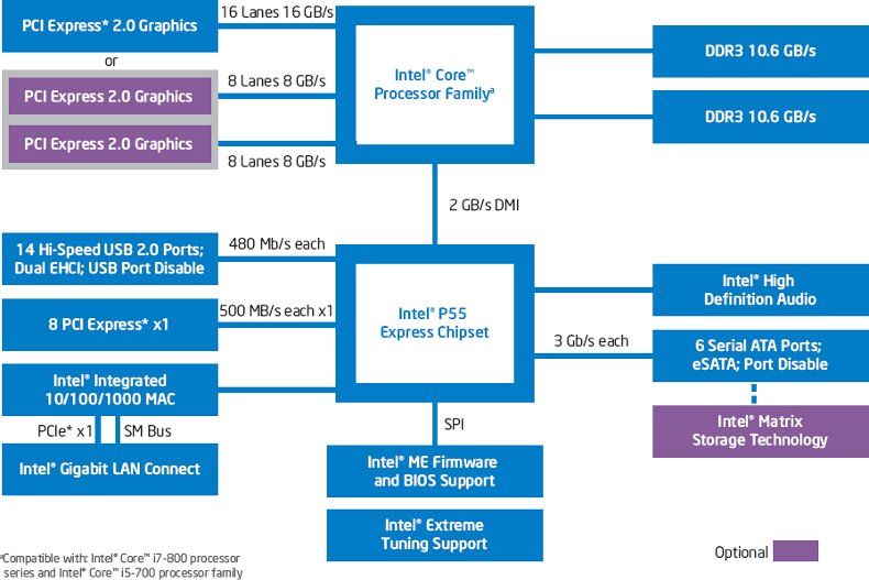
October 2009, at the same time that the output of I5, Intel seems to go back, resuming the former external bus QDI and socket LPGA1156 for series 8XX. As I5, it include PCI-Express (but not the chipset). The only difference with the I5, it include again hypertreading
17. Intel I5.
In 2009, Intel with the I7 is more processor performance desktop market (even if the price is rather a game specialist). However, AMD catfish market share on the part below. Intel released in October 2009 the I5 (with some models I7 as explained above). The external bus is therefore in DMI but keeping the structure of its big brother (except hyperthreading but keeping the turbo mode with overclocking a bit lower).
Second difference, a PCI-Express card display is directly integrated into the processor (but not the P55 witch is the chipset associate). Finally, I5 manages the DDR3 too but in Dual Channel.
| The continuation of the hardware 1 course > 5.A. Dedicated processors Servers - 6. Internal bus for PC |
The hardware 1 course: PC and peripherals. The Hardware 2 course: networks, servers and communications